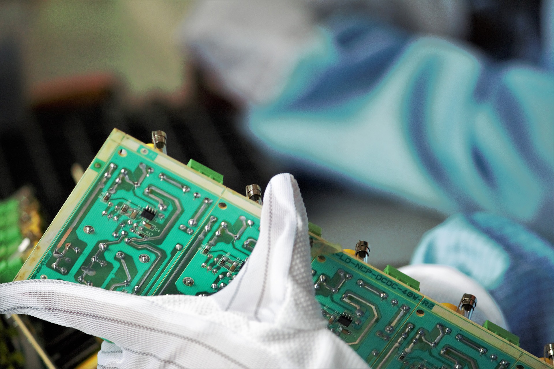
PCB panel design process requires some special consideration. First define the purpose of the panel. Plan early to increase the SMT production efficiency. There should be extra breakaway rails and sufficient space on the panel to avoid components conflicting or going over the PCB edges. Pay attention to the strength and mechanical stability. The panel should be able to withstand the stress during the assembly and production processes.
The ease of assembling and manufacturability are important characteristics and requirements for panel production. The border should be minimum 5 mm. Copper elements and holes should not be placed close to the PCB edge. The minimum distance between the element and the V-cut lines should be 0.4 mm. Many breakout tabs should be inserted on a routed panel and placed in both X and Y directions. An efficient design prevents panel damage during the production process.
