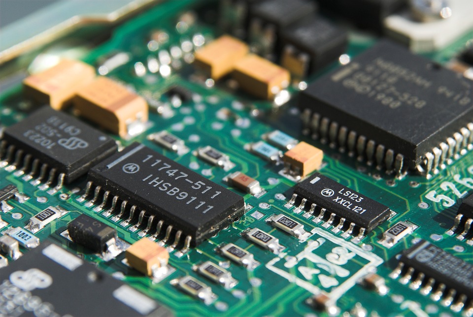
Multi-layer PCB is one of the most popular PCB types in use today. It offers many advantages over traditional single-layer PCBs and is used in various applications. This article will discuss the basics of Multi-layer PCBs and some of their benefits.
Multi-layer PCBs consist of multiple layers of conductive material, typically alternating between insulating and conductive layers. This allows for more circuitry to be packed into a smaller space and provides better electrical insulation between different circuit parts. Multi-layer PCBs can have anywhere from two to twelve or more layers.
Multi-layer PCBs are used in various electronic devices, from cell phones and laptops to industrial control systems. They are also used in many medical devices and military applications. Multi-layer PCBs offer several benefits over traditional single-layer PCBs, including:
- Increased density: They can pack more circuitry into a smaller space than single-layer PCBs.
- Improved electrical performance: They can provide better electrical insulation between different circuit parts, allowing for shorter trace lengths and lower impedance.
- Enhanced mechanical stability: They are less likely to warp or flex than single-layer PCBs, making them more resistant to mechanical stress. Multi-layer PCBs offer many advantages over single-layer PCBs, including increased circuit density, enhanced mechanical stability, and improved signal integrity. However, they are also more complex to manufacture and more expensive. When considering which type of PCB to use for your next project, weigh the pros and cons of each option to decide which is best for your needs.


